- 您现在的位置:买卖IC网 > Sheet目录1998 > ICS844004AK-104LF (IDT, Integrated Device Technology Inc)IC SYNTHESIZER LVDS 32-VFQFPN
ICS844004-104
FEMTOCLOCKCRYSTAL-TO-LVDS FREQUENCY SYNTHESIZER
IDT / ICS LVDS FREQUENCY SYNTHESIZER
10
ICS844004AK-104 REV. A SEPTEMBER 15, 2008
Recommendations for Unused Input and Output Pins
Inputs:
LVCMOS Control Pins
All control pins have internal pulldowns; additional resistance is not
required but can be added for additional protection. A 1k
resistor
can be used.
REF_CLK INPUT
For applications not requiring the use of the reference clock,
it can be left floating. Though not required, but for additional
protection, a 1k
resistor can be tied from the REF_CLK to
ground.
Outputs:
LVDS Outputs
All unused LVDS output pairs can be either left floating or
terminated with 100
across. If they are left floating, we
recommend that there is no trace attached.
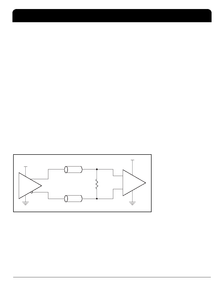
3.3V, 2.5V LVDS Driver Termination
A general LVDS interface is shown in Figure 4. In a 100
differential transmission line environment, LVDS drivers require a
matched load termination of 100
across near the receiver input.
For a multiple LVDS outputs buffer, if only partial outputs are used,
it is recommended to terminate the unused outputs.
Figure 4. Typical LVDS Driver Termination
LVDS Driver
R1
100
–
+
50
50
3.3V or 2.5V
V
DD
100
Differential Transmission Line
发布紧急采购,3分钟左右您将得到回复。
相关PDF资料
ICS844004AKI-104LFT
IC SYNTHESIZER LVDS 32-VFQFPN
ICS844021BG-01LFT
IC CLOCK GEN ETHERNET 8-TSSOP
ICS844021BGI-01LFT
IC CLOCK GEN ETHERNET 8-TSSOP
ICS844071AGLFT
IC CLOCK GEN GIG ETH 8-TSSOP
ICS844201BG-45LF
IC CLK GENERATOR 25MHZ 8TSSOP
ICS844204BK-245LF
IC CLK SYNTHESIZER 4LVDS 32VFQFN
ICS844S42BKILF
IC SYNTHESIZER RF FREQ 56-VFQFPN
ICS86004BG-01LF
IC CLK BUFFER ZD 1:4 16-TSSOP
相关代理商/技术参数
ICS844004AK-104LFT
功能描述:IC SYNTHESIZER LVDS 32-VFQFPN RoHS:是 类别:集成电路 (IC) >> 时钟/计时 - 时钟发生器,PLL,频率合成器 系列:HiPerClockS™, FemtoClock™ 标准包装:1,000 系列:- 类型:时钟/频率合成器,扇出分配 PLL:- 输入:- 输出:- 电路数:- 比率 - 输入:输出:- 差分 - 输入:输出:- 频率 - 最大:- 除法器/乘法器:- 电源电压:- 工作温度:- 安装类型:表面贴装 封装/外壳:56-VFQFN 裸露焊盘 供应商设备封装:56-VFQFP-EP(8x8) 包装:带卷 (TR) 其它名称:844S012AKI-01LFT
ICS844004AKI-104LF
功能描述:IC SYNTHESIZER LVDS 32-VFQFPN RoHS:是 类别:集成电路 (IC) >> 时钟/计时 - 时钟发生器,PLL,频率合成器 系列:HiPerClockS™, FemtoClock™ 标准包装:2,000 系列:- 类型:PLL 频率合成器 PLL:是 输入:晶体 输出:时钟 电路数:1 比率 - 输入:输出:1:1 差分 - 输入:输出:无/无 频率 - 最大:1GHz 除法器/乘法器:是/无 电源电压:4.5 V ~ 5.5 V 工作温度:-20°C ~ 85°C 安装类型:表面贴装 封装/外壳:16-LSSOP(0.175",4.40mm 宽) 供应商设备封装:16-SSOP 包装:带卷 (TR) 其它名称:NJW1504V-TE1-NDNJW1504V-TE1TR
ICS844004AKI-104LFT
功能描述:IC SYNTHESIZER LVDS 32-VFQFPN RoHS:是 类别:集成电路 (IC) >> 时钟/计时 - 时钟发生器,PLL,频率合成器 系列:HiPerClockS™, FemtoClock™ 标准包装:1,000 系列:- 类型:时钟/频率合成器,扇出分配 PLL:- 输入:- 输出:- 电路数:- 比率 - 输入:输出:- 差分 - 输入:输出:- 频率 - 最大:- 除法器/乘法器:- 电源电压:- 工作温度:- 安装类型:表面贴装 封装/外壳:56-VFQFN 裸露焊盘 供应商设备封装:56-VFQFP-EP(8x8) 包装:带卷 (TR) 其它名称:844S012AKI-01LFT
ICS844004BGI-01LF
功能描述:IC SYNTHESIZER 4LVDS 24-TSSOP RoHS:是 类别:集成电路 (IC) >> 时钟/计时 - 时钟发生器,PLL,频率合成器 系列:HiPerClockS™, FemtoClock™ 标准包装:27 系列:Precision Edge® 类型:频率合成器 PLL:是 输入:PECL,晶体 输出:PECL 电路数:1 比率 - 输入:输出:1:1 差分 - 输入:输出:无/是 频率 - 最大:800MHz 除法器/乘法器:是/无 电源电压:3.135 V ~ 5.25 V 工作温度:0°C ~ 85°C 安装类型:表面贴装 封装/外壳:28-SOIC(0.295",7.50mm 宽) 供应商设备封装:28-SOIC 包装:管件
ICS844004BGI-01LFT
功能描述:IC SYNTHESIZER 4LVDS 24-TSSOP RoHS:是 类别:集成电路 (IC) >> 时钟/计时 - 时钟发生器,PLL,频率合成器 系列:HiPerClockS™, FemtoClock™ 标准包装:27 系列:Precision Edge® 类型:频率合成器 PLL:是 输入:PECL,晶体 输出:PECL 电路数:1 比率 - 输入:输出:1:1 差分 - 输入:输出:无/是 频率 - 最大:800MHz 除法器/乘法器:是/无 电源电压:3.135 V ~ 5.25 V 工作温度:0°C ~ 85°C 安装类型:表面贴装 封装/外壳:28-SOIC(0.295",7.50mm 宽) 供应商设备封装:28-SOIC 包装:管件
ICS844008AKI-46LF
功能描述:IC CLK GEN 8LVDS 32-VFQFPN RoHS:是 类别:集成电路 (IC) >> 时钟/计时 - 时钟发生器,PLL,频率合成器 系列:HiPerClockS™, FemtoClock™ 标准包装:2,000 系列:- 类型:PLL 频率合成器 PLL:是 输入:晶体 输出:时钟 电路数:1 比率 - 输入:输出:1:1 差分 - 输入:输出:无/无 频率 - 最大:1GHz 除法器/乘法器:是/无 电源电压:4.5 V ~ 5.5 V 工作温度:-20°C ~ 85°C 安装类型:表面贴装 封装/外壳:16-LSSOP(0.175",4.40mm 宽) 供应商设备封装:16-SSOP 包装:带卷 (TR) 其它名称:NJW1504V-TE1-NDNJW1504V-TE1TR
ICS844008AKI-46LFT
功能描述:IC CLK GEN 8LVDS 32-VFQFPN RoHS:是 类别:集成电路 (IC) >> 时钟/计时 - 时钟发生器,PLL,频率合成器 系列:HiPerClockS™, FemtoClock™ 标准包装:1,000 系列:- 类型:时钟/频率合成器,扇出分配 PLL:- 输入:- 输出:- 电路数:- 比率 - 输入:输出:- 差分 - 输入:输出:- 频率 - 最大:- 除法器/乘法器:- 电源电压:- 工作温度:- 安装类型:表面贴装 封装/外壳:56-VFQFN 裸露焊盘 供应商设备封装:56-VFQFP-EP(8x8) 包装:带卷 (TR) 其它名称:844S012AKI-01LFT
ICS844008AY-16LF
功能描述:IC CLOCK GEN 8LVDS 32PTQFP RoHS:是 类别:集成电路 (IC) >> 时钟/计时 - 时钟发生器,PLL,频率合成器 系列:HiPerClockS™, FemtoClock™ 标准包装:2,000 系列:- 类型:PLL 频率合成器 PLL:是 输入:晶体 输出:时钟 电路数:1 比率 - 输入:输出:1:1 差分 - 输入:输出:无/无 频率 - 最大:1GHz 除法器/乘法器:是/无 电源电压:4.5 V ~ 5.5 V 工作温度:-20°C ~ 85°C 安装类型:表面贴装 封装/外壳:16-LSSOP(0.175",4.40mm 宽) 供应商设备封装:16-SSOP 包装:带卷 (TR) 其它名称:NJW1504V-TE1-NDNJW1504V-TE1TR